


견고한 인쇄 회로 기판

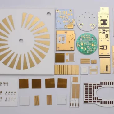
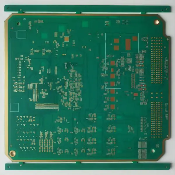
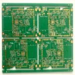
Rigid circuit board is the most common and primary electronic component to a PCB assembly. Rigid PCB can be manufactured into single layer, double layers and multi-layer designs. There are also a wide range of materials which they can be manufactured with low cost to high technology.
Availbe for Production Order, Hot Order, Qucik Turn PCBS: Small volume prototype, Quick-turn pre-production circuit boards,Production quick-turn circuit boards
- 설명
- 매개변수
설명
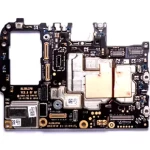
Rigid PCB
Rigid PCB circuit consists of conducting layers made of copper foil and insulating layers dielectric that are typically laminated together with epoxy resin prepreg. The board is typically coated with solder mask.

We build thousands of different products for our customers across a wide range of technologies and applications.

우리의 기술 역량은 다음과 같습니다. 90% 모든 PCB 기술의. 간단히 말하면, 우리는 거의 모든 PCB를 잘 만들 수 있습니다.
표면 마감

우수한 품질
- 들어오는 품질 관리
유명 브랜드의 원료를 사용하고 있습니다., 국제 및 고객 표준을 준수하는 수입 자재 검사 규정을 확립했습니다., 공급업체의 품질 개선 활동을 지속적으로 추적하고 홍보합니다., 공급업체와 강력한 협력관계를 구축하고 유지합니다..
- 공정 품질 관리
작업 사양 및 작업 표준이 올바르게 구현되도록 생산 라인의 각 프로세스에 대한 표준화된 생산 프로세스 및 세부 작업 지침을 제공합니다..
- 완제품 품질 관리
우리는 국제 표준 및 고객 표준에 따라 배송 품질을 엄격하게 확인하고 관리합니다., 선적 후 제품 품질 성능에 대한 적시 후속 조치, 고객에 대해 신속하고 효과적인 개선 조치를 취합니다.


| Feature | 매개변수 | |
| 레이어 | 1 – 36L | |
| Max Board Size | 580 x 1080mm, advanced 610 x 1400mm | |
| Board Thickness Range | 0.40 – 7.0mm | |
| Copper weight | 18 – 210μm, advanced 1050μm / 30oz | |
| Min Line Width /Space | 2.5 밀 / 2.5 밀 | |
| Minimum mechanical drill | 0.20 mm | |
| Minimum laser drill | 0.10mm 표준, 0.075mm advanced | |
| PTH Wall Thickness | 1 밀 | |
| PTH Dia. Tolerance | ± 3 밀 | |
| NPTH hole Dia. Tolerance | ± 2 밀 | |
| Hole Position Deviation | ±2 mil | |
| Layer Registration | ≥ 4mil | |
| Outline Tolerance | ± 4 밀 | |
| S/M Pitch | 3 밀 | |
| 종횡비 | 18:1 | |
| Warp & Twist | ≤0.7% | |
| Solder Mask Abrasion | ≥ 6H | |
| Flammability | 94다섯-0 | |
| Impedance Control | Diff >50ohm | +/- 10% |
| Single-end ≤50 ohm | +/- 8% | |
| HDI Capability | Any Layer | |
| Dimple | 20하나, 10um advanced | |
| Back Drill Size min | 0.40mm | |
| Special Technology | POFV | 예 |
| Hybrid Lamination | 예 | |
| Metallized half hole | 예 | |