")


Гибкие и жестко-гибкие ПЕЧАТНЫЕ ПЛАТЫ

Flex PCB, also known as FPC (flexible printed circuit board), is a circuit board which utilizes plastic substrates, like polyimide or polyester films, to create a flexibly and durable material for assembling components. FPC can be connection points or the primary control board of a PCB assembly.
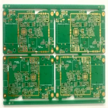
Rigid-Flex PCB combines the features of rigid and flexible into one PCB. The rigid portion provides durability and the flexible section provides light weight a thin profile for various applications.
- Описание
- Параметры
Описание
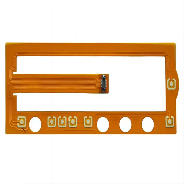
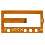
Flexible Printed Circuit (ФПК)
Flexible printed circuit consists of conducting layers made of copper foil and insulating layers dielectric that are typically laminate together with polyimide / PET / PEN / Liquid Crystal Polymer (LCP).
The board is used as a substrate for assembling electronics devices and can be bent for specific applications.
Single Side FPC
- Consists of a single conductor layer of metal or conductive polymer on a flexible dielectric film.
- Component termination features are accessible only from one side, with holes in the base film for component assembly.

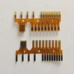
Double Side FPC
- Consists of 2 conductive layers fabricated with or without plated through holes.
- When constructed without plated through hole, the connection features are accessible only from one side.
- Because of the plated through hole, terminators for electronics components are provided on both sides of the circuit, allowing components to be placed on either side.

Multi Layered Flex Circuit
- Consists of 3 or more layers of conductive and are also known as multilayer flex circuit.
- Layers are interconnected by plated through hole or openings to access lower circuit level features.
- Discontinuous lamination is common in cases that require maximum flexibility or bending.

Bare Backed Flex Circuit
- Bare Back Flex Circuit (double access) has a single conductor layer that allows access to features of the conductor pattern such as lead termination from both sides.
- This is not commonly manufactured because of the special processing required to provide access to the features discretely.

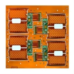
Rigid Flex Circuit
- Hybrid constructions consists of flexible and rigid substrates are laminated together into a single structure and then electrically interconnected using plated through hole.


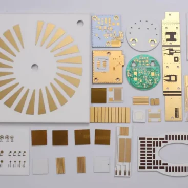
We build thousands of different products for our customers across a wide range of technologies and applications.

Наши технологические возможности охватывают более 90% всех технологий печатных плат. Проще говоря, мы можем хорошо собрать практически любую печатную плату. Please refer to parameters
Surface Finishes

Отличное качество
- Входной контроль качества
Используем сырье известных брендов., установили правила входного контроля материалов, соответствующие международным стандартам и стандартам клиентов, постоянно отслеживать и продвигать деятельность поставщиков по улучшению качества, а также строить и поддерживать тесное сотрудничество с поставщиками.
- Контроль качества процесса
Стандартизированный производственный процесс и подробные инструкции по эксплуатации для каждого процесса производственной линии, обеспечивающие правильное соблюдение эксплуатационных характеристик и стандартов эксплуатации..
- Контроль качества готовой продукции
Мы строго проверяем и контролируем качество отгрузки в соответствии с международными стандартами и стандартами клиентов., Своевременное отслеживание качества продукции после отгрузки, и предпринимать быстрые и эффективные действия по улучшению работы клиента


| ЭЛЕМЕНТ | Спецификация | Comments | |
| Layer counts | Flexible PCB | 1-10 Слои | |
| Rigid-Flex PCB | 2-16 Слои | ||
| HDI PCB | 2+N+2 Layers | ||
| Copper Thickness | 6um min | ||
| 4OZ max | |||
| PNL Size(maximum) | 610*914мм | ||
| Hole Diameter | Laser drilling | 0.05мм мин. | |
| Mechanical drilling | 0.15мм мин. | ||
| Hard tooling Hole | 0.50мм | ||
| Aspect Ratio(maximum) | Through hole | 10:1 | |
| Blind hole | 2:1 | ||
| Line (minimum) | 1/3oz Copper | 1.2мил | LDI |
| 0.5oz Copper | 1.5мил | ||
| 0.5oz Copper | 2мил | Film exposure | |
| 1oz Copper | 3мил | ||
| 2oz Copper | 4мил | ||
| Измерение&Tolerances | Hole Size | ± 0,05 мм | H≦2.0mm |
| Line | ±10% | W≧0.25mm | |
| Accumulate tolerance | ± 0,05 мм | Вт<0.25мм | |
| Line to outline | ± 0,05 мм | P≦25mm | |
| Outline tolerance | ± 0,05 мм | C≦5.0mm | |
| Impedance tolerance | ±10% | ||
| Connectivity test | Resistance(minimum) | 0.5мОм | Four lines |
| Resistance(minimum) | 5Ой | Ordinary | |
| Insulation Resistance | 50MΩ | Ordinary | |