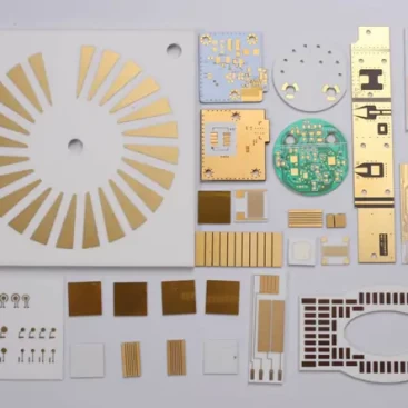


RIGID PRINTED CIRCUIT BOARDS

Rigid circuit board is the most common and primary electronic component to a PCB assembly. Rigid PCB can be manufactured into single layer, double layers and multi-layer designs. There are also a wide range of materials which they can be manufactured with low cost to high technology.
Availbe for Production Order, Hot Order, Qucik Turn PCBS: Small volume prototype, Quick-turn pre-production circuit boards,Production quick-turn circuit boards
- Description
- PARAMETERS
Description
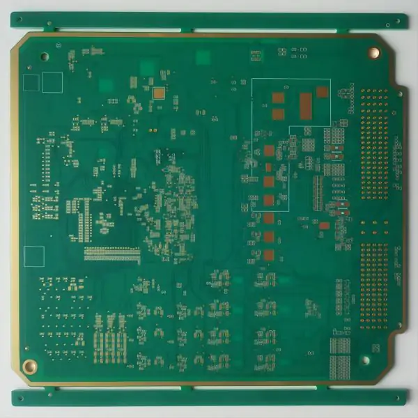
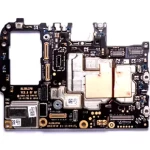
Rigid PCB
Rigid PCB circuit consists of conducting layers made of copper foil and insulating layers dielectric that are typically laminated together with epoxy resin prepreg. The board is typically coated with solder mask.

We build thousands of different products for our customers across a wide range of technologies and applications.

Our technology capability covers over 90% of all PCB technologies. Simply stated, we can build almost any PCB well.
Surface Finishes

Excellent Quality
- Incoming Quality Control
We use raw materials from famous brands, have established incoming material inspection regulations that comply with international and customer standards, constantly trace and promote supplier quality improvement activities, and build and maintain strong cooperation with suppliers.
- Process quality control
Standardized production process and detailed operation instructions for each process of the production line to ensure that the operation specifications and operation standards are correctly implemented.
- Finished product quality control
We strictly check and control the shipment quality according to the international standards and customer standards, timely follow up the product quality performance after shipment, and take quick and effective improvement actions on the customer


| Feature | Parameter | |
| Layers | 1 – 36L | |
| Max Board Size | 580 x 1080mm, advanced 610 x 1400mm | |
| Board Thickness Range | 0.40 – 7.0mm | |
| Copper weight | 18 – 210μm, advanced 1050μm / 30oz | |
| Min Line Width /Space | 2.5 mil / 2.5 mil | |
| Minimum mechanical drill | 0.20 mm | |
| Minimum laser drill | 0.10mm standard, 0.075mm advanced | |
| PTH Wall Thickness | 1 mil | |
| PTH Dia. Tolerance | ± 3 mil | |
| NPTH hole Dia. Tolerance | ± 2 mil | |
| Hole Position Deviation | ±2 mil | |
| Layer Registration | ≥ 4mil | |
| Outline Tolerance | ± 4 mil | |
| S/M Pitch | 3 mil | |
| Aspect Ratio | 18:1 | |
| Warp & Twist | ≤0.7% | |
| Solder Mask Abrasion | ≥ 6H | |
| Flammability | 94V-0 | |
| Impedance Control | Diff >50ohm | +/- 10% |
| Single-end ≤50 ohm | +/- 8% | |
| HDI Capability | Any Layer | |
| Dimple | 20um, 10um advanced | |
| Back Drill Size min | 0.40mm | |
| Special Technology | POFV | Yes |
| Hybrid Lamination | Yes | |
| Metallized half hole | Yes | |